Scanning Electron Microscopes (SEM)
Scanning electron microscopes (SEM) represent a cornerstone technology in modern laboratory microscopy, enabling researchers to visualize materials and biological specimens at unprecedented resolutions. These sophisticated scanning electron microscope instruments utilize focused electron beams to create detailed surface images that reveal structural features down to the nanometer scale. Unlike conventional light microscopes limited by wavelength constraints, scanning electron microscope machines harness the shorter wavelengths of accelerated beam of electrons to achieve resolutions ranging from sub-nanometer to 20 nanometers, depending on the scanning electron microscope model.read more
The versatility of SEM instrument makes them indispensable across diverse scientific disciplines, from materials science and nanotechnology to life sciences and forensic analysis. Modern SEM systems feature advanced capabilities including variable accelerating voltages (0.3 kV to 30 kV), multiple detector configurations, and automated image acquisition functions that streamline workflow efficiency. Whether selecting a compact scanning electron microscope for teaching laboratories or an high-resolution scanning electron system for advanced research, understanding the key features and applications of these instruments is essential for making informed purchasing decisions.
Key Features
Scanning electron microscope features vary significantly across different models, but several core capabilities define their imaging performance and operational flexibility.
- High-resolution imaging capabilities: The best scanning electron microscope models deliver secondary electron resolutions between 0.4 nm and 3.0 nm at 30 kV accelerating voltage, with some systems achieving resolutions below 1 nm. Low-voltage performance typically ranges from 10-15 nm at 1-3 kV, enabling examination of beam-sensitive materials.
- Versatile magnification range: Modern scanning electron microscope instruments offer magnification from as low as ×5 up to ×3,000,000, with typical systems providing ×5 to ×300,000 for standard imaging applications and extended ranges for specialized research.
- Multiple detector configurations: SEM systems incorporate secondary electron detectors for topographical imaging and backscattered electron detectors for compositional contrast, with resolutions of 4.0 nm at 30 kV for backscattered electrons. Advanced models may include energy dispersive X-ray spectroscopy (EDS) integration for elemental analysis.
- Variable operating modes: Scanning electron microscopes SEM feature high-vacuum, low-vacuum, and environmental scanning modes to accommodate diverse specimen types, with low-vacuum settings ranging from 6 to 650 Pa.
- Flexible accelerating voltage control: Adjustable voltages from 0.3 kV to 30 kV enable optimization of imaging parameters based on specimen characteristics and desired information depth. This wide voltage range supports both surface-sensitive imaging at low energies and high-resolution imaging at elevated voltages.
- Automated operation functions: Contemporary scanning electron microscope types incorporate auto-focus control (AFC), auto brightness and contrast control (ABCC), auto stigma and focus (ASF), and auto beam alignment (ABA) to streamline operation and ensure consistent imaging quality.
- Advanced specimen stage systems: Five-axis motorized stages provide precise specimen positioning with X and Y axes travel ranges up to 150 mm, Z-axis movement from 5-85 mm, continuous 360° rotation, and tilt capabilities from -20° to +90°.
Applications of Scanning Electron Microscopes
Scanning electron microscope lab applications span numerous scientific and industrial sectors, where nanoscale imaging and surface characterization are critical.
- Materials science characterization: Scanning electron microscopes allow detailed investigation of material properties, composition, and microstructure across aerospace, energy, chemistry, and electronics industries. Researchers utilize SEM for studying high-temperature superconductors, mesoporous architectures, and alloy strength characteristics that drive material development.
- Nanomaterials research: SEM technology provides essential insights into nanotubes, nanofibres, and other nanoscale structures, supporting innovation in nanotechnology and advanced materials engineering.
- Quality control and failure analysis: Manufacturing sectors employ scanning electron microscope instruments for routine quality assessment, defect identification, and failure mode analysis to ensure product reliability and performance standards.
- Biological and life sciences imaging: Research laboratories utilize SEM for examining cellular structures, tissue morphology, and biomaterial interfaces at resolutions that reveal ultrastructural details critical for understanding biological processes.
- Forensic science investigations: Specialized scanning electron microscope models support forensic applications including trace evidence analysis, material identification, and surface feature documentation for investigative purposes.
- Semiconductor and microelectronics inspection: The semiconductor industry relies on SEM for examining integrated circuit features, analyzing fabrication defects, and measuring critical dimensions at nanometer scales.
Showing 1–12 of 28 results
Category
- Bioreactors+
- Parallel Bioreactors
- Single-Use Bioreactors
- Stirred-Tank Bioreactors
- Capillary Electrophoresis Instruments+
- Capillary Gel Electrophoresis (CGE)
- Capillary Isoelectric Focusing (CIEF)
- Capillary Zone Electrophoresis (CZE)
- Cell Counters and Analyzers+
- Automated Cell Counters
- Manual Cell Counters
- Cellular Imaging Systems+
- Fluorescence Imaging Systems
- High-Content Imaging Systems
- Live-Cell Imaging Systems
- Centrifuges+
- Benchtop Centrifuges
- Clinical Centrifuges
- Micro Centrifuges
- Refrigerated Centrifuges
- Ultracentrifuges
- Chromatography Instruments+
- Gas Chromatography
- Ion Chromatography
- Liquid Chromatography
- Flow Cytometer+
- Cell Analyzers
- Cell Isolation Systems
- Cell Sorters
- High-Throughput Flow Cytometers
- Imaging Flow Cytometry
- Personal Flow Cytometers
- Portable/Benchtop Flow Cytometers
- Spectral Flow Cytometers
- Laboratory Incubators+
- CO2 Incubators
- Dry Bath Incubators
- Hypoxia Incubators and Chambers
- Incubator Shakers
- Laboratory Ovens
- Portable Incubators
- Thermal Mixers
- Laboratory Microscopes+
- Atomic Force Microscopes (AFM)
- Automated Modular Microscopes
- Compound Microscopes
- Confocal Microscopes
- Digital Microscopes
- Fluorescence Microscopes
- Inverted Microscopes
- Live Cell Imaging Microscopes
- Metallurgical Microscopes
- Multiphoton Microscopes
- Polarizing Microscopes
- Raman Microscopes
- Scanning Electron Microscopes (SEM)
- Stereo Microscopes
- Super-Resolution Microscopes
- Transmission Electron Microscopes (TEM)
- Upright Microscopes (Neuroscience)
- Liquid Handlers+
- Automated Pipetting Systems
- Multi-Channel Liquid Handlers
- Robotic Liquid Handlers
- Variable Volume Pipetting Systems
- Mass Spectrometers+
- Ambient Ionization
- APCI MS
- ESI MS
- FT ICR MS
- ICP MS
- Orbi Trap MS
- Quadrupole MS
- Time-of-Flight MS
- Microarray Scanners+
- DNA Microarray Scanners
- Laser-Based Microarray Scanners
- Microplate Readers+
- Absorbance Microplate Readers
- Fluorescence Microplate Readers
- Luminescence Microplate Readers
- Multimode Microplate Readers
- Particle Counters and Analyzers+
- Airborne Particle Counters
- Laser Diffraction Analyzers
- Liquid Particle Counters
- Nanoparticle Analyzers
- Portable Particle Counters
- Remote Particle Counters
Brand
- ACCU-SCOPE
- Agilent
- Airmodus
- Alphasense
- Analytik Jena
- ARGO-HYTOS
- Arrayit
- Aurora Biomed Inc.
- Azure Biosystems
- Baker
- BD Biosciences
- Beckman Coulter
- Beijing Challen Biotechnology
- Binder
- Bio-Techne
- Biobase
- BioRad
- BMG Labtech
- Bruker
- Celestron
- Cellbox
- Centurion Scientific Ltd
- ChemoMetec
- CleanAir
- Cleatech
- Corning
- Countstar
- CS Instruments
- CUBIC
- Cytek Biosciences
- Cytena
- Cytiva
- Data Technologies
- Descase
- Electrolab Biotech
- Eppendorf
- Euromex
- Evident
- Fermex
- Fluke
- Formulatrix
- Getinge
- Gilson
- GPC Bio
- Haier Biomedical
- Hamilton Company
- Hettich
- Hitachi High-Tech
- Hudson Robotics Inc.
- Hydro
- INFORS HT
- Innopsys
- Jasco
- Jeiotech
- JEOL
- Kanomax
- Keyence
- KNAUER
- LAB-KITS
- Labomed
- Labwit
- Leco
- Leica
- Lighthouse
- Logos Biosystems
- LOSI
- Lumex Instruments
- Luminex
- Malvern Panalytical
- Meiji Techno
- Memmert
- Merck
- Mettler-Toledo International Inc.
- Miltenyi Biotec
- Molecular Devices
- Motic
- MP Filtri
- MSE (Medical and Scientific Equipment)
- NCI
- Nikon Instruments
- NuAire
- ORFLO Technologies
- Oxford Instruments
- PAMAS
- Particle Measuring Systems
- Particles Plus
- PBS Biotech
- PCE instruments
- PerkinElmer
- PharSol
- PHCbi
- Prior Scientific
- Promega
- Qiagen NV
- Revvity
- RION
- Sartorius
- SATAKE
- Sciex
- Sebia
- SETA
- Setra
- Shimadzu
- SIBATA
- Sigma Laborzentrifugen GmbH
- Solaris Biotech
- Solida Biotech
- Sony Biotechnology Inc.
- SPT Labtech Ltd
- Stratedigm Inc.
- Sysmex Corporation
- Tecan
- TES
- Thermo Fisher Scientific
- TSI
- Waters
- Western States Machine Company
- ZEISS
- ZETRON
-

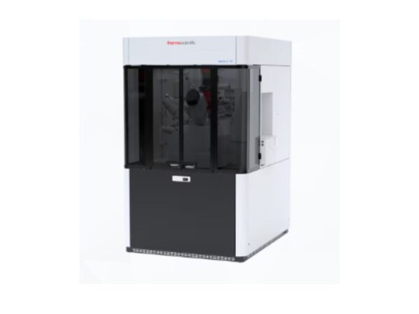
Thermo Fisher Scientific Apreo 2 SEM
Apreo SEM delivers exceptional resolution, contrast, and versatility for demanding research and QA tasks.
-

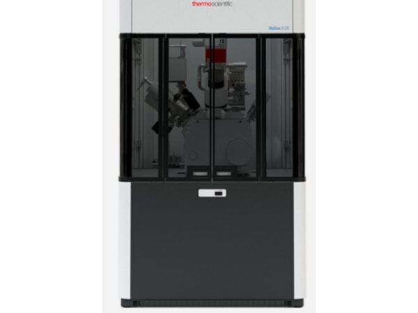
Thermo Fisher Scientific Aquilos 2 Cryo-FIB
Aquilos Cryo-FIB combines SEM and FIB technologies for superior imaging and sample preparation workflows.
-

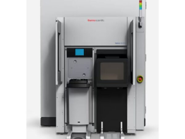
Thermo Fisher Scientific Arctis Cryo Plasma-FIB
Arctis Cryo-PFIB integrates advanced TEM technology with automated features for top-quality nanoscale analysis.
-

Thermo Fisher Scientific Axia ChemiSEM
Axia ChemiSEM offers intuitive SEM operation with simultaneous chemical and structural imaging capabilities.
-

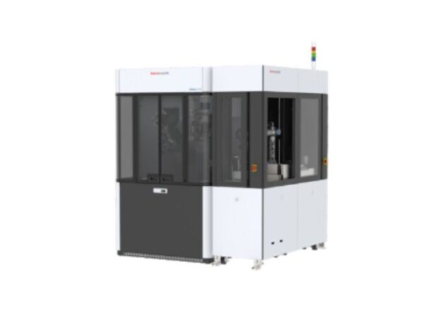
Thermo Fisher Scientific FIB-SEM and Laser Ablation
FIB-SEM with Laser Ablation combines SEM and FIB technologies for superior imaging and sample preparation workflows.
-
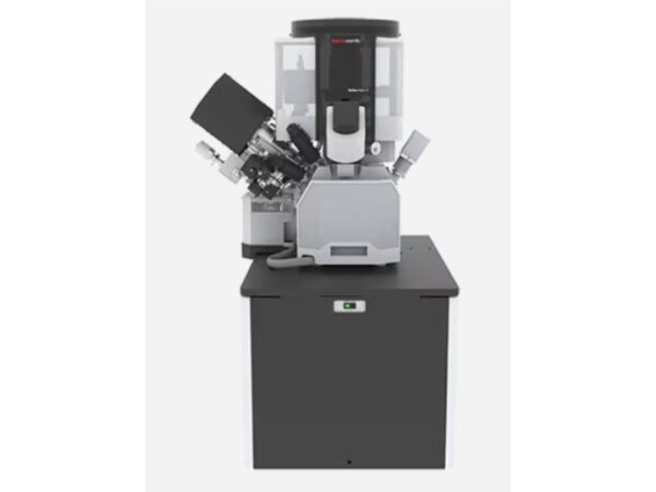
Thermo Fisher Scientific Helios 5 DualBeam
Helios 5 DualBeam combines SEM and FIB technologies for superior imaging and sample preparation workflows.
-
Thermo Fisher Scientific Helios 5 EXL DualBeam
Helios 5 EXL DualBeam combines SEM and FIB technologies for superior imaging and sample preparation workflows.
-
Thermo Fisher Scientific Helios 5 Hydra DualBeam
Helios Hydra DualBeam combines SEM and FIB technologies for superior imaging and sample preparation workflows.
-
Thermo Fisher Scientific Helios 5 PFIB DualBeam
Helios 5 PFIB DualBeam combines SEM and FIB technologies for superior imaging and sample preparation workflows.
-
Thermo Fisher Scientific Helios 6 HD FIB-SEM
Helios 6 HD DualBeam combines SEM and FIB technologies for superior imaging and sample preparation workflows.
-
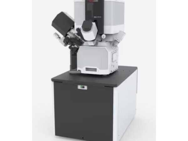
Thermo Fisher Scientific Helios 6 HX FIB-SEM
Helios 6 HX enables high-resolution SEM/FIB operations with smart automation and analytical capabilities.
-

Thermo Fisher Scientific Helios 6 HXS FIB-SEM
Helios 6 HXS offers ultra-high resolution imaging with precise FIB milling and sample analysis.